
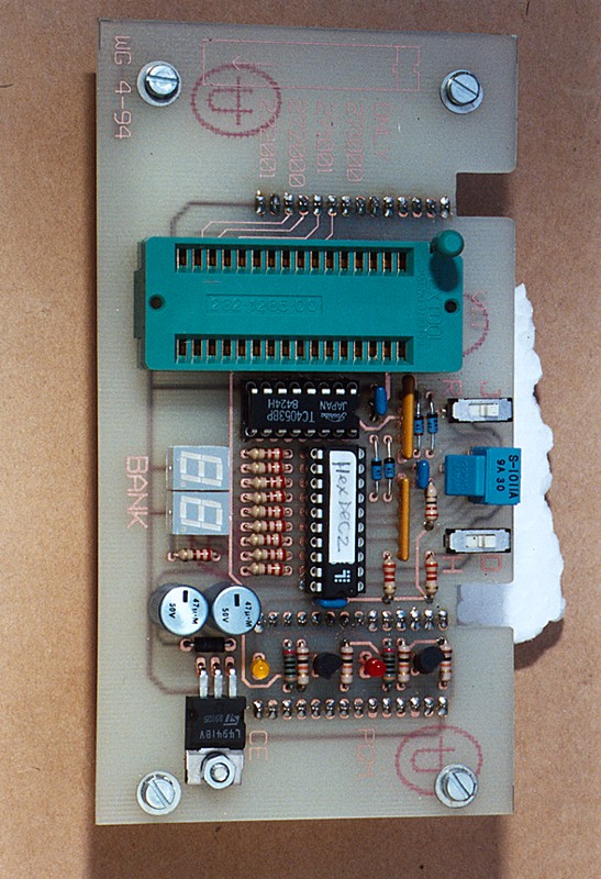
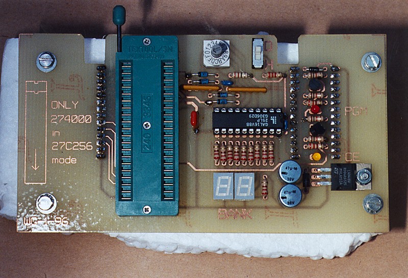
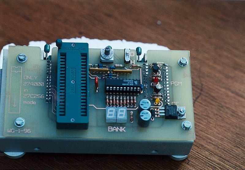
            SUNSHINE EPROM PROGRAMMER CARD : EW-904BN(new model)

1.0 REVISION OF EW-904 series :
    MODEL EW-904,904A: have been faded out at 1986,servicing only.
                       I/O BASE ADDRESS is 3C0.
                       Software V1.0 to V5.7 is old style menu.
                       Software V6.0 or greater is new style menu.
                       More powerful than old software.

    MODEL EW-904B    : have been faded out,servicing only.
                       I/O BASE ADDRESS is 390.
                       Software V1.0 to V5.7 is old style menu.
                       Software V6.0 or greater is new style menu.
                       More powerful than old software.

    MODEL EW-904BN   : available at end of FEB 1989(new model).
                       I/O BASE ADDRESS is 2A0.
                       Software V7.0 is almost the same as V6.0.
                       We add a built in screen editor that is more friendly
                       than DOS DEBUG.COM.

                       Because we apply some filter circuit on test socket
                       BOX and interface card,  the CMOS EPROM problems
                       are solved on this model.
                       CMOS EPROM can be programmed by general NMOS EPROM
                       programming algo., except that the NS CMOS EPROM
                       has to be programmed by its own algo.

                            NOTE
     EW-904BN is not compatible with EW-904B on software and hardware.
| A0 cycle | 8088 XT-8MHz | 386DX40 in XT-mode | 286-16 | 386SX-16 | 386SX-33 | 386DX-40 | 486DX2-66 |
| /CE or /OE after A0 | 8088 XT 8MHz 1st --- 2nd |
386DX40 in XT mode 1st --- 2nd |
286-16 1st --- 2nd |
386SX-16 1st --- 2nd |
386SX-33 1st --- 2nd |
386DX-40 1st --- 2nd |
486DX2-66 1st --- 2nd |
| 904B | 78 --- 116 | 65 --- 100 | 17.5 --- 27 | 18 --- 28 | 12 --- 18 | 6 --- 10.5 | 5 --- 8 |
| 904BN | 58 | 50 | 14 | 14 | 7.5 | 5.5 | 2 |
| IMAGE FILE | |
| foto14.jpg | Miniature view of the MAX626 circuit with wires and capacitors attached to it |
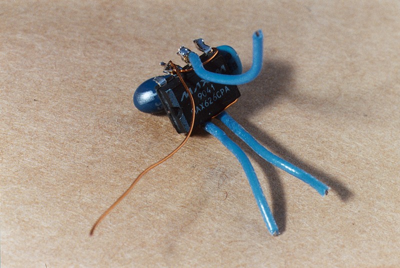
| foto15.jpg | Larger view of the MAX626 circuit, other side, with wires attached. |
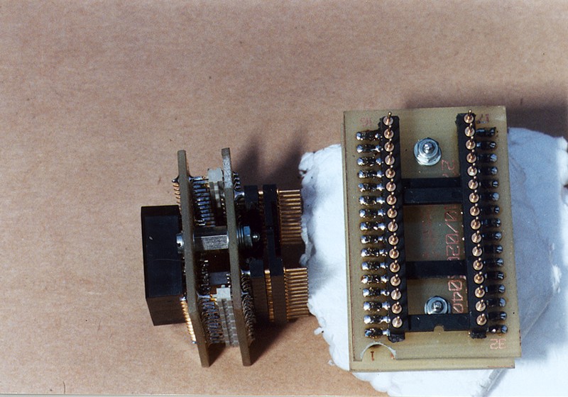
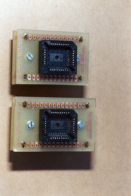
| foto16.jpg | PLCC adapters, with side view of the sandwich construction |
| foto17.jpg | EW904B total component side view, all modifications: I/O290, earth loop correction, TL497 circuit, some pull-up R's, Vpp pull down R's and the A13 modification. A mess, but works great. |
| foto18.jpg | EW904B view zoomed in on the component side, all modifications: I/O290, earth loop correction, TL497 circuit, and A13 modification are visible. |
| foto19.jpg | EW904B view zoomed in on the solder side, all modifications: I/O290, earth loop correction, TL497 circuit, and A13 modification |
| foto20.jpg | Top (component) side of the 27C1000/2000 adapter |
| foto21.jpg | Only earth loop modification wire TL 497 circuit, emitter Q4 to common earth point C5 |
| foto22.jpg | Top (component) side of the 27C4000 adapter |
| foto23.jpg | Top (component) side angle view of the 274000 adapter |
| foto24.jpg | 27C4000 adapter solder side view. The 27C1000/2000 version looks allmost the same. Mounting construction of the sockets and pin-pin adapter |
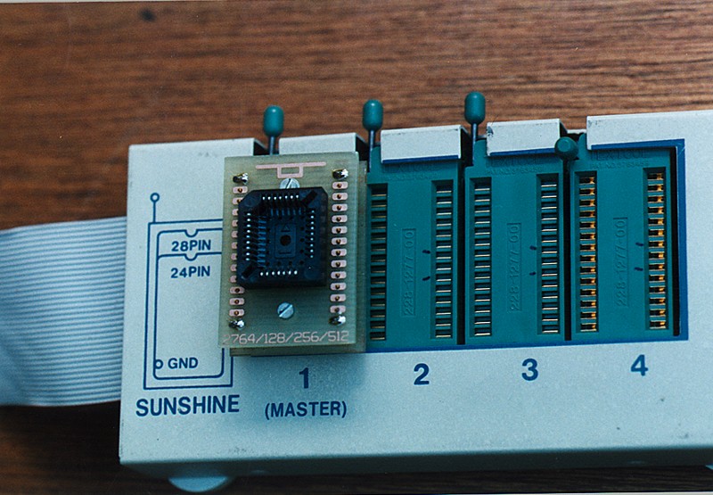
| foto25.jpg | PLCC adapter on top of the ZIF unit |
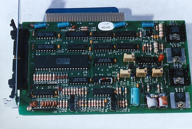
| foto26.jpg | Component side EW904BN board, notice: yellow wire databus diode near mounting bracket, diode changes Vpp, coil oscillation damp components, multiturn pots in place of original pots, and the A13 pull-up R. |
| foto28.jpg | PLCC adapters |
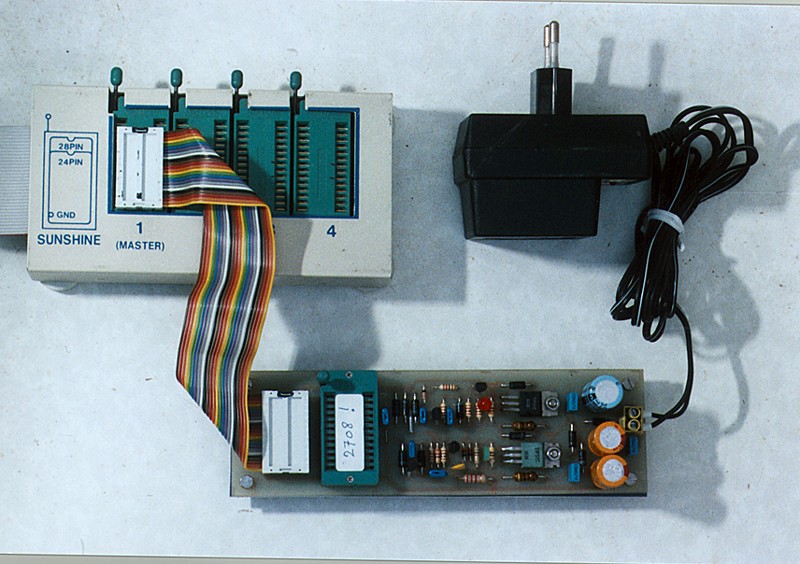
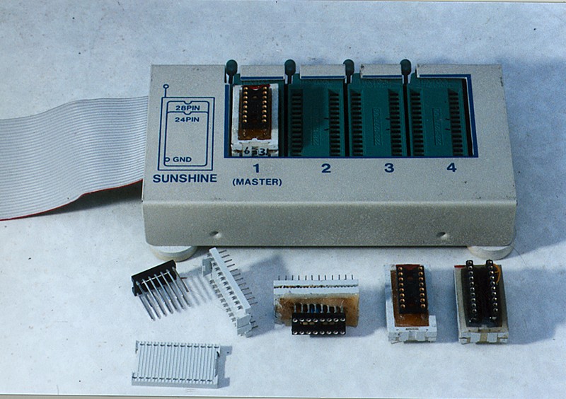
| foto30.jpg | 2708 read only construction / adapter with power supply / transformer |
| foto31.jpg | TTL prom readout adapters plus construction example (a reverse engineering aid). DIL plug as mounting base, wire-wrap socket (pins partly cut) placed inside, wiring with wirwrap wire and solder. Some epoxy resin to stabilise. |
| GIF FILE | PROGRAMMER | CIRCUIT | |
| 904B-T | EW904B | TL497 | Vpp = 25 volt out, also for all other related curves. Original start situation, circuit is in error. Timing wrong mainly due to parasitic feedback. TIP31C becomes hot. |
| 904B-U | EW904B | TL497 | Parasitic feedback problems solved. ONE ground wire added and an extra buffer electrolyte. No RC or by-pass D yet added, no D's changed. Lots of "bumping". If the bump hits zero, current becomes negative. See positive dips in current curve. |
| 904B-S (904B-1) | EW904B | TL497 | Almost finished. RC damping added and a by-pass switch diode. Normal 1N4002 rectifier still in place. |
| 904B-V | EW904B | TL497 | Difference with -S is switch rectifier RGP10M in place of 1N4002. See the difference in switch off ringing. Doesn't it look nice now?? Like in datasheet books? Current is swinging nice in and out... And the TIP31C doesn't become (too) hot anymore. |
| 904BN-W (904BN-OK) | EW904BN | TL497 | The circuit itself is unchanged, it is OK. The diodes are both changed by switch versions, and a damping network was added. |
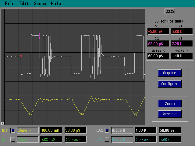
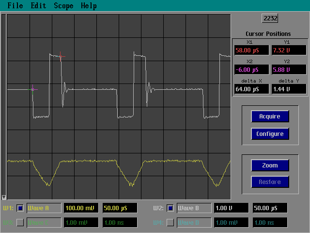
| A13-OFF | EW904B | A13 | A13 ON and OFF with the former 1 uF speedup-C. Works great but the looks are not neat. |
| A13-ON | EW904B | A13 | A small dip under and overshoot. Watch timing scale: 50usec/div. 5usec/div would have been more appropriate. I didn't realised then it was that worse! |
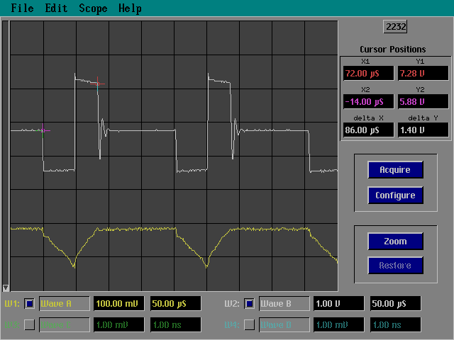
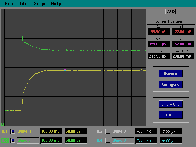
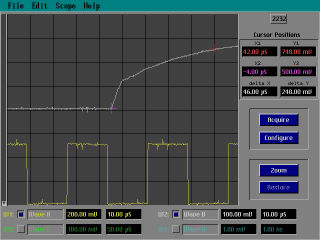
| A13-BN | EW904BN | A13 | Original rise time is the slowest 300 usec one!!! |
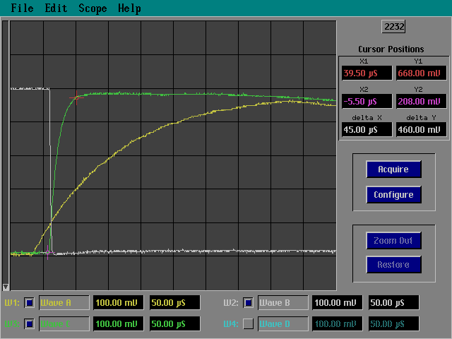
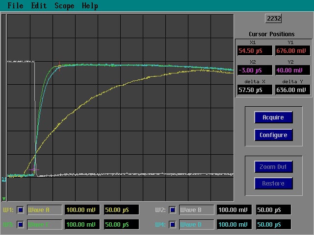
| A13-BN2 | EW904BN | A13 | Fall time is reasonable (could be better). The faster rise time is with 470 Ohm pull-up. The fastest is with 330 Ohm, still not fast enough. 220 Ohm is used now, that's the allowable safe min. The circuit is still begging for more speed....... |
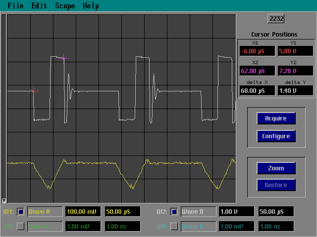
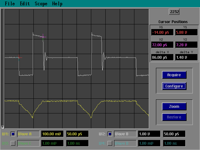
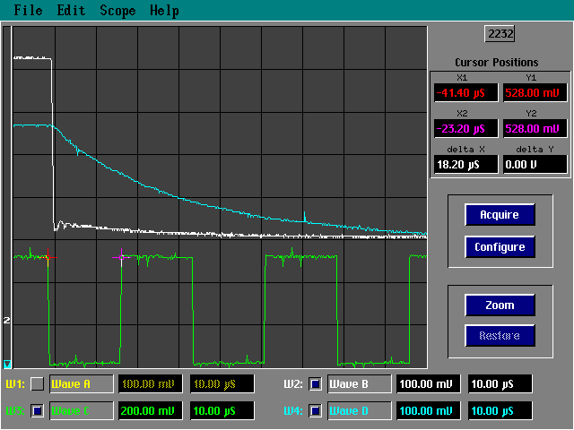
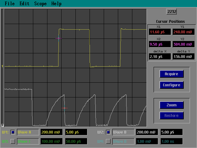
| 904BA13A | EW904B | A13 | A more appropriate comparison: A13 falltime compared with the A0 cycle time on a 386SX-33 (= 18 usec). And now at 10usec/div. |
| 904BA13B | EW904B | A13 | And this is the A13 rise time compared with 18usec A0. |
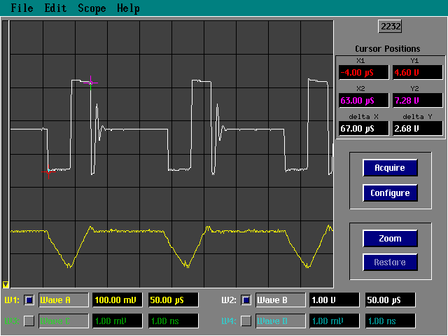
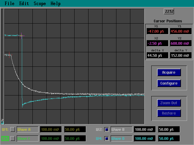
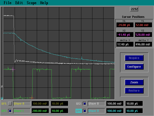
| 904BA13C (904BA13E) | EW904B | A13 | This is the improved A13 circuit falltime with A0 cycle and original circuit timings combined. There is one thing changed now: the speedup-C = 150 nF, we are reaching zero very neat, but is slowly creeping to exactly zero. A 0.2 Volt improvement is with a 180nF speedup-C inplace of the 150nF. |
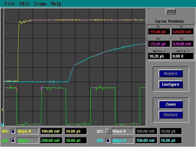
| 904BA13D | EW904B | A13 | This is the risetime pulse, original and improved. The original slow rise has been shifted to the right. It starts original at the same point (centre-trigger was chosen). |
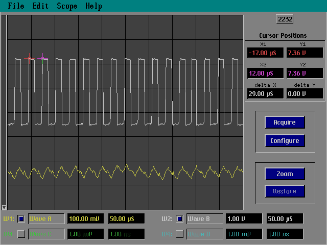
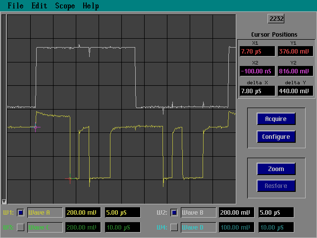
| 904B-CE2 904B-CE | EW904B | /CE | Both showing /CE pulses with 18 or 21 usec A0 timing false (?) pulse and real /CE pulse. |
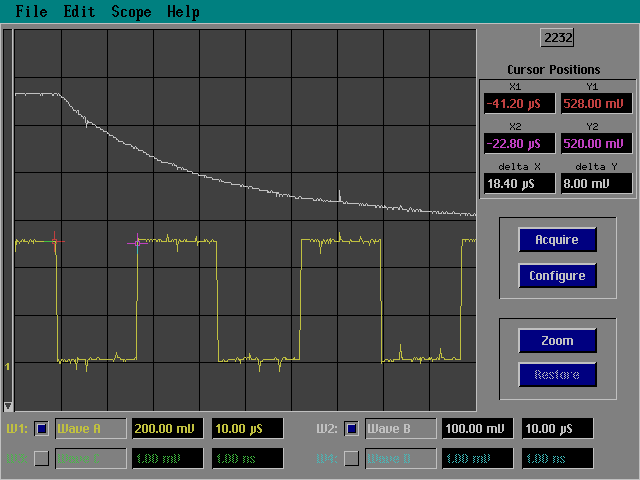
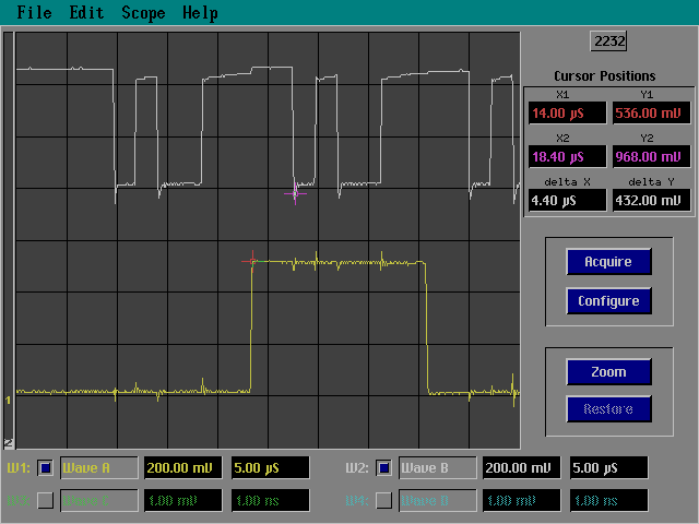
| 904BN-OE | EW904BN | /OE | On the 904BN version the software is even running faster. Only 11 to 12 usec A0 timing (486DX2-66). And this file shows how tricky the timing is. |
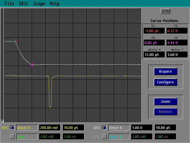
| 904B-VPP | EW904B | Vpp | This is the timing for a jump from 21 to 5V Vpp during programming. Vpp delay is 12 usec. /CE is 12 usec further. That looks OK for the CPU speed of that moment. (taken from a ... machine) |
 Back to Sunshine
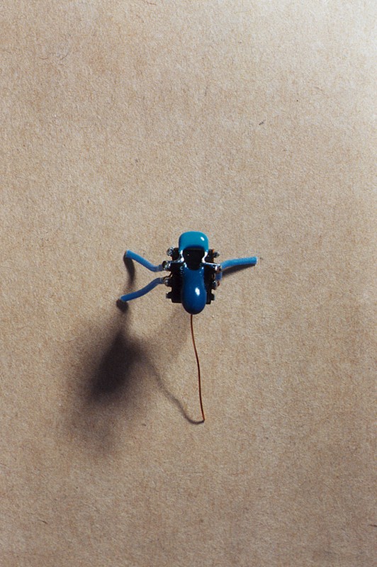